I2C Master Controller in VHDL
Introduction
This project implements a finite state machine-based I2C master controller to interface a Xilinx Artix-7 FPGA with peripheral microcontrollers. The core engineering challenge was managing the protocol’s bidirectional open-drain signaling and dynamic timing requirements without relying on a static clock divider.
Hardware & Constraints
The target hardware is a Digilent Cmod A7-35T FPGA. The system is driven by a 12 MHz system clock with a period of 83.33 ns. To meet the I2C standard, SCL and SDA lines must be held high or low for a minimum of 5.0µs. At 12 MHz, this requires a timer to count 60 clock cycles after the physical line transition actually completes. Furthermore, SDA transitions are constrained to occur at least 2.5µs (30 clock cycles) after an SCL transition completes.
System Architecture
The design is modularized into a top-level wrapper, a graphical user interface (GUI) UART handler, and the core I2C controller.
- I/O Buffering: To handle open-drain bidirectional signaling and bypass Vivado power-on initialization limitations, Xilinx
IOBUFprimitives are instantiated at the top level to explicitly separate input (sda_in,scl_in) and output (sda_out,scl_out) paths. - FSM and Clock Stretching: The datapath is governed by a cycle-accurate FSM handling Start, Address, Read/Write, Data, Acknowledge, Repeated Start, and Stop conditions. The FSM implements clock stretching by dynamically polling the input buffers (e.g., waiting for
scl_into read ‘1’) before initializing the 5.0µs delay counters, ensuring compliance regardless of bus capacitance.
Verification Strategy
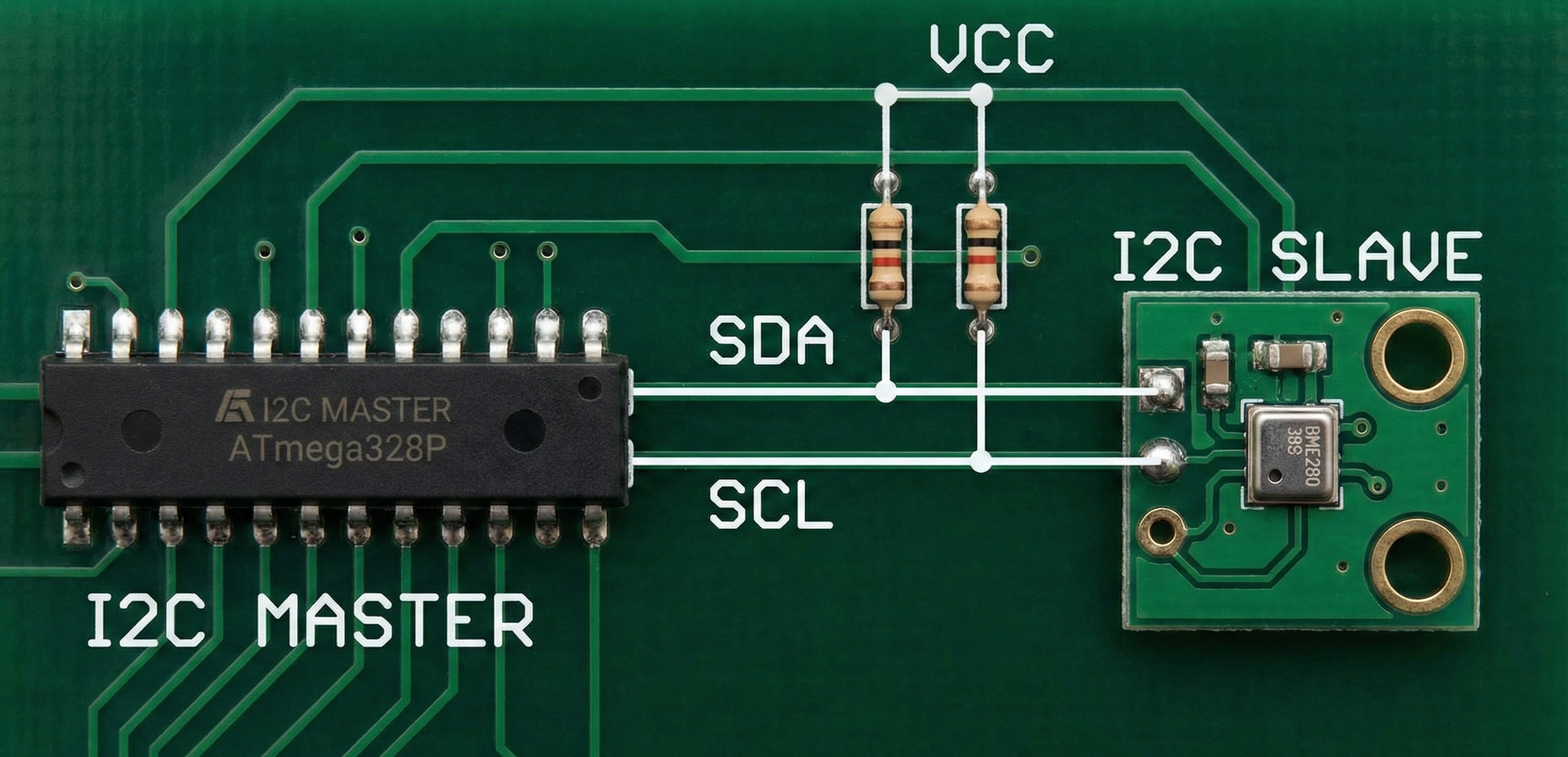
The RTL logic was verified via simulation testbenches prior to synthesis. The simulation environment instantiates the device under test (DUT) and drives the open-drain SCL and SDA lines to a weak high ('H') to accurately model the physical pull-up resistors on the I2C bus. This allows the master to pull the bus low and verify that the lines correctly float back to a high state during idle and acknowledge periods.
Hardware-in-the-Loop Testing
The synthesized bitstream was loaded onto the FPGA and interfaced with a PIC16F18326 microcontroller acting as the I2C slave. A MATLAB GUI running on a host PC transmitted 8-bit payloads over UART to the FPGA. The FPGA forwarded the payload to the PIC via I2C, received a translated response byte, and returned it to the MATLAB GUI to confirm end-to-end timing and protocol compliance in hardware.
Conclusion
Implementing this protocol from scratch reinforced the necessity of cycle-accurate timing analysis and the careful management of asynchronous inputs in digital logic design.
The full VHDL source code, self-checking testbenches, and Xilinx Vivado constraints for this project can be found on my GitHub repository.